- 您现在的位置:买卖IC网 > Sheet目录251 > SGN08G64B3BB2SA-CCWRT (Swissbit NA Inc)SDRAM DDR3 8GB 204 SO-DIMM
�� �
�
�preliminary� Data� Sheet�
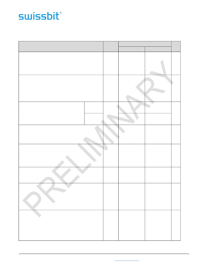
�I� DD� Specifications� and� Conditions�
�(0°C� ≤� T� CASE� ≤� +� 85°C;� V� DDQ� =� +1.5V� ±� 0.075V,� V� DD� =� +1.5V� ±� 0.075V)�
�Rev.0.9�
�15.11.2011�
�Parameter�
�&� Test� Condition�
�OPERATING� CURRENT� *)� :�
�One� device� bank� Active-Precharge;�
�Symbol�
�I� DD0�
�max.�
�12800-11-11-11�
�480�
�10600-9-9-9�
�440�
�Unit�
�mA�
�t� RC� =� t� RC� (I� DD� );� t� CK� =� t� CK� (I� DD� );� CKE� is� HIGH,� CS#� is� HIGH�
�between� valid� commands;�
�DQ� inputs� changing� once� per� clock� cycle;� Address� and�
�control� inputs� changing� once� every� two� clock� cycles�
�OPERATING� CURRENT� *)� :�
�One� device� bank;� Active-Read-Precharge;�
�I� DD1�
�560�
�520�
�mA�
�I� OUT� =� 0mA;� BL� =� 4,� CL� =� CL� (I� DD� ),� AL� =� 0;�
�t� CK� =� t� CK� (I� DD� ),� t� RC� =� t� RC� (I� DD� ),� t� RAS� =� t� RAS� MIN� (I� DD� ),�
�t� RCD� =� t� RCD� (I� DD� );� CKE� is� HIGH,� CS#� is� HIGH� between�
�valid� commands;� Address� inputs� changing� once� every�
�two� clock� cycles;� Data� Pattern� is� same� as� I� DD4W�
�PRECHARGE� POWER-DOWN�
�CURRENT:�
�Slow� Exit�
�I� DD2P�
�240�
�240�
�mA�
�All� device� banks� idle;� Power-down� mode;�
�t� CK� =� t� CK� (I� DD� );� CKE� is� LOW;� All� Control� and� Fast� Exit�
�Address� bus� inputs� are� not� changing;� DQ’s�
�are� floating� at� V� REF�
�240�
�240�
�PRECHARGE� QUIET� STANDBY� CURRENT:�
�All� device� banks� idle;�
�I� DD2Q�
�320�
�320�
�mA�
�t� CK� =� t� CK� (I� DD� );� CKE� is� HIGH,� CS#� is� HIGH;�
�All� Control� and� Address� bus� inputs� are� not� changing;�
�DQ’s� are� floating� at� V� REF�
�PRECHARGE� STANDBY� CURRENT:�
�All� device� banks� idle;�
�I� DD2N�
�400�
�400�
�mA�
�t� CK� =� t� CK� (I� DD� );� CKE� is� HIGH,� CS#� is� HIGH;�
�All� other� Control� and� Address� bus� inputs� are� changing�
�once� every� two� clock� cycles;� DQ� inputs� changing� once�
�per� clock� cycle�
�ACTIVE� POWER-DOWN� CURRENT:�
�I� DD3P�
�320�
�320�
�mA�
�All� device� banks� open;� t� CK� =� t� CK� (I� DD� );� CKE� is� LOW;� All�
�Control� and� Address� bus� inputs� are� not� changing;� DQ’s�
�are� floating� at� V� REF� (always� fast� exit)�
�ACTIVE� STANDBY� CURRENT:�
�All� device� banks� open;� t� CK� =� t� CK� (I� DD� ),�
�I� DD3N�
�480�
�480�
�mA�
�t� RAS� =� t� RAS� MAX� (I� DD� ),� t� RP� =� t� RP� (I� DD� );�
�CKE� is� HIGH,� CS#� is� HIGH� between� valid� commands;�
�All� other� Control� and� Address� bus� inputs� are� changing�
�once� every� two� clock� cycles;� DQ� inputs� changing� once�
�per� clock� cycle�
�OPERATING� READ� CURRENT:�
�All� device� banks� open,� Continuous� burst� reads;� One�
�I� DD4R�
�920�
�800�
�mA�
�module� rank� active;� I� OUT� =� 0mA;� BL� =� 4,� CL� =� CL� (I� DD� ),�
�AL� =� 0;� t� CK� =� t� CK� (I� DD� ),� t� RAS� =� t� RAS� MAX� (I� DD� ),� t� RP� =� t� RP�
�(I� DD� );� CKE� is� HIGH,� CS#� is� HIGH� between� valid�
�commands;� Address� bus� inputs� are� changing� once�
�every� two� clock� cycles;� DQ� inputs� changing� once� per�
�clock� cycle�
�Swissbit� AG�
�Industriestrasse� 4�
�CH� –� 9552� Bronschhofen�
�Fon:� +41� (0)� 71� 913� 03� 03�
�Fax:� +41� (0)� 71� 913� 03� 15�
�www.swissbit.com�
�eMail:� info@swissbit.com�
�Page� 7�
�of� 15�
�发布紧急采购,3分钟左右您将得到回复。
相关PDF资料
SGN08G72G1BB2SA-CCWRT
SDRAM DDR3 8GB 204 SO-UDIMM
SGP1200-12G
FRONT END AC/DC 1133W 12V
SL05.TCT
TVS ARRAY DATA INTFC SOT-23
SL24T1G
TVS LO CAP 300W 24V ESD SOT23
SLD10U-022-B
DIODE TVS AXIAL HI-POWER
SLP-2-413-01
SNAP LOCK PINS TEAR-DROP .413"
SLVU2.8-4.TBT
IC TVS ARRAY 4-LINE 2.8V 8SOIC
SLVU2.8-8.TBT
IC TVS ARRAY 8-LINE 2.8V 8SOIC
相关代理商/技术参数
SGN08G64B3BB2SA-DCRT
制造商:SWISSBIT 功能描述:DDR3 SO-DIMM 8 GB 1600/CL11 - Trays 制造商:SWISSBIT NA INC 功能描述:DDR3 8GB SODIMM 制造商:Swissbit 功能描述:DIMM / SO-DIMM / SIMM DDR3, SO-DIMM, 8 GB, 1600/CL11, 0 C to + 70 C
SGN08G64B3BB2SA-DCWRT
制造商:SWISSBIT NA INC 功能描述:DDR3 8GB SODIMM 制造商:Swissbit 功能描述:DIMM / SO-DIMM / SIMM 8GB DDR3 SDRAM 64 bit SO-DIMM CL11
SGN08G72G1BB2SA-CCWRT
功能描述:SDRAM DDR3 8GB 204 SO-UDIMM RoHS:是 类别:存储卡,模块 >> 存储器 - 模块 系列:- 标准包装:100 系列:- 存储器类型:SDRAM 存储容量:1GB 速度:133MHz 特点:- 封装/外壳:168-DIMM
SGN08G72G1BB2SA-DCRT
制造商:SWISSBIT 功能描述:DDR3 SO-DIMM 8 GB 1600/CL11 - Trays 制造商:SWISSBIT NA INC 功能描述:DDR3 8GB SODIMM
SGN08G72G1BB2SA-DCWRT
功能描述:MODULE DDR3 SDRAM 8GB 204SOUDIMM 制造商:swissbit na inc. 系列:- 零件状态:过期 存储器类型:DDR3 SDRAM 存储容量:8GB 速度:1600MT/s 封装/外壳:204-SO-UDIMM 标准包装:100
SGN2M056TG
制造商:Panasonic Industrial Company 功能描述:DOOR
SGN72288FH8P6PH
制造商:SMART Modular Technology Inc 功能描述:MEMORY MODULE - Trays
SGN72568FH8P0PH
制造商:SMART Modular Technology Inc 功能描述:ECC 256MX8 .94" DDR3-1333 NVDIMM - Trays